 Researchers from the University of Illinois at Urbana-Champaign have developed a new way to form 3-D shapes from flat, 2-D sheets of graphene, paving the way for future integrated systems of graphene-MEMS hybrid devices and flexible electronics. “To the best of our knowledge, this study is the first to demonstrate graphene integration to a variety of different microstructured geometries, including pyramids, pillars, domes, inverted pyramids, and the 3D integration of gold nanoparticles (AuNPs)/graphene hybrid structures,” explained SungWoo Nam, an assistant professor of mechanical science and engineering at Illinois. “The flexibility and 3D nature of our structures will enable intimate biosensing devices which can be conformed to the shape and characteristics of human skin and other biological systems. The 3D protruding micro-structures can also achieve enhanced sensitivity by maximizing the effective contact area between the sensors and non-flat surfaces.
“We also expect that our new 3D integration approach will facilitate advanced classes of hybrid devices between microelectromechanical systems (MEMS) and 2D materials for sensing and actuation.”
Graphene, a two-dimensional honeycomb lattice of sp2-bonded carbon atoms, has been widely studied due to its high carrier mobility, chemical inertness, and biocompatibility. To date, various reported methods of graphene transfer have been mostly limited to planar or curvilinear surfaces due to the challenges associated with fractures from local stress during transfer onto 3D microstructured surfaces.
“Our method utilizes wet-transfer and adaptive substrate-engineering, providing several key advantages over other fabrication/integration methods of 3D graphene,” stated Jonghyun Choi, a graduate student in Nam’s research group and first author of the article, “Three-Dimensional Integration of Graphene via Swelling, Shrinking, and Adaptation,” appearing in Nano Letters. “Our results demonstrate a simple, versatile, and scalable method to integrate graphene with 3D geometries with various morphologies and dimensions. Not only are these 3D features larger than those reported in previous works, but we also demonstrate the uniformity and damage-free nature of integrated graphene around the 3D features.”
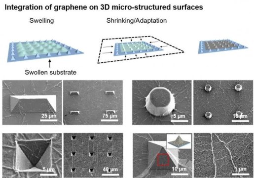
The researchers’ robust approach to integrate graphene onto 3D microstructured surfaces maintains the structural integrity of graphene, where the out-of-plane dimensions of the 3D features vary from 3.5 to 50 μm. The process incorporates three sequential steps: 1) substrate swelling using a solvent that 2) shrinks during the evaporation process, allowing graphene to 3) adapt, or conform to the shape of a prepared substrate, to achieve damage-free, large area integration of graphene on 3D microstructures.
“Our swelling, shrinking, and adaptation steps are optimized to minimize the degree of graphene suspension around the 3D microstructures and facilitate successful 3D integration,” Nam added. “We control the amount of substrate swelling by adjusting the time of immersion in organic solvent and the mixing ratios of monomer and curing agent of the polydimethylsiloxane (PDMS) substrate.”
Detailed scanning electron microscopy, atomic force microscopy, Raman spectroscopy, and electrical resistance measurement studies show that the amount of substrate swelling, as well as the flexural rigidities of the transfer film, affect the integration yield and quality of the integrated graphene. To demonstrate the versatility of their approach, the researchers applied the process to a variety of 3D microstructured geometries, as well as integrating hybrid structures of graphene decorated with gold nanoparticles onto 3D microstructure substrates, demonstrating the compatibility of the integration method with other hybrid nanomaterials.
In addition to Nam and Choi, the article’s co-authors include Hoe Joon Kim, Michael Cai Wang, Juyoung Leem, and William P. King, from the Department of Mechanical Science and Engineering at Illinois.
This work was supported by the Air Force Office of Scientific Research/Asian Office of Aerospace Research Development Nano Bio Info Technology (NBIT) Phase III Program, the American Chemical Society Petroleum Research Fund, the Korean-American Scientists and Engineers Association and the National Science Foundation. Experiments were carried out in part in the Frederick Seitz Materials Research Laboratory and the Micro and Nano Technology Laboratory, and the Beckman Institute Imaging Technology Group at Illinois.


