Materials and ecology are today’s challenges. Coatings are not excluded: nanotechnology coatings meet the industry’s requirements in innovative manner.
What is the role of coating? Generalizing, we can state that in consists in conferring particular properties and/or characteristics, both functional and aesthetical, to the surface of a manufactured item (or to a part of it). Typically, thanks to the coating action, it is possible to improve the resistance to wear, to corrosion, to friction ad so on, but also “decorative” effects can be achieved, like the colouring or the texture. In addition to standard coatings, interesting solutions come from the nano world, including all those materials and systems that have at least one of the dimensions included between 1 and 100 nanometres; the material handling, performed through processes that allow a complete control of composition and structure, permit to attain different properties, new and improved, compared to those of massive materials. A typical problem concerns parts in motion, where the wear is the priority requisite: to increase the resistance to wear of a surface, it is fundamental to decrease the friction among the parts. Nanotechnology satisfies this as well as several other needs, developing coatings able to reduce friction through the combination of an isotropic finish and an opportune deposition, in the order of nanometres, which fills the depressions caused by the residual roughness, meanwhile granting an excellent resistance to scratch, delamination and a good lubricating power.
The nanometric coating
If the coating is a classic concept, nowadays the coating typology is undergoing a notable evolutionary boost. Today are increasingly diffused the nanotechnology coatings, able to confer extremely varied functional characteristics to the treated surfaces, which can be of almost any material and shape. The most common are the resistance to corrosion, the easy to clean, the water- and oleo- repellence, the anti-scratch, the anti-fog, the anti-bacteria; interesting are also the applications providing for the anti-fingerprint, the anti-graffiti, but also the anti-counterfeiting. The first applications of the coating based on nanotechnologies were in civil engineering, especially in the coating of façades of structures particularly exposed to aggressive atmospheric environments, such as the zones with high traffic intensity, and then they gradually extended to all product sectors. Nanometric coatings are durable and invisible, they do not modify the substrate aspect, with the exception of specific needs, they allows elastic deformations and, in some cases and within certain limits, also plastic ones; they can be applied on almost any material, from metal to polymeric alloys, with consolidated and relatively simple application processes. Generally, surface treatments according to nanotechnology criteria allow achieving materials with particular surface properties, without anyway needing a particular care of the properties of the entire material, since the only surface is called to perform a determinate task. The most common examples include the products for aesthetical applications, products with surfaces resistant to abrasion and to corrosion, products with high hydrophobicity/hydrophilicity properties, with specific optical specifications, like the anti-glare or the anti-scratch, etc.: the surface satisfies the demanded requisites and not the entire mass of material. Nanotechnology coatings are frequently called “with nanometric thickness “, owing to the coating thickness, which is in the order of microns: the properties that the treated surface can reach are achievable also by an extremely low quantity of precursors.
Processes
Nowadays, the productive technologies for nanotechnology coatings are different, but two in particular seem to arouse the market’s interest, to the extent that the most popular are the so-called PE-CVD coatings and sol-gel coatings. The processes that exploit the PE-CVD technology, acronym of Plasma Enhanced Chemical Vapor Deposition, are efficient and relatively cheap, usable on any substrate, from metals to ceramic or polymeric materials. PE-CVD processes, which exploit vacuum plasma, are scalable, environmentally sustainable and they allow obtaining homogeneous and very adherent coatings, easily adapted to different shapes, characterized by specific properties such as anti-corrosion, anti-adherence, anti-wear, anti-scratch, hydrophobicity, oleophobicity and so on. Operationally, the PE-CVD coating process occurs in vacuum chambers; precursors are vaporized and activated at the plasma state; condensing on the substrate surface, they form coating films with high adhesion and uniform distribution. Since the process occurs at a temperature under 100°C, this technology, opportunely optimized, can be used also on thermo-sensitive materials. The Sol Gel technology allows attaining coating films applicable on all substrate types, according to the sol used: through a control on nanometric scale of the various oxides, it is possible to achieve, at low cost, extremely diversified products and applications. In particular, the industrial applications of sol gel coatings can concern hydrophilic and self-cleaning surfaces, photocatalytic devices, anti-bacteria surfaces, fabrics with release of essences and medicines, anti-scratch surfaces and so on. The process starts from organometallic or inorganic precursors in solution that, through hydrolysis and condensation processes, form colloidal solutions, the sols, of metal oxide particles; after the sol deposition, the gel formation occurs, still through hydrolysis and condensation processes. Eventual successive drying and/or solidification treatments allow eliminating the liquid gel phase, in order to enhance the mechanical characteristics.
Nanoparticles in coatings?
They are not real nanotechnology coatings, with almost inexistent thicknesses, but the presence of nanoparticles in coatings represents a highly innovative application of nanotechnologies, in line with the requirements of environment protection. The use of potentially dangerous materials for man, both during the production phase of the good and, in the long term, in its use, urges the legislator towards regulations, or at least recommendations, hindering its use. Chrome, one of the most used both as anti-corrosive and as functional coating, is certainly one of the most debated substances and they try to set some limits to its use. Currently, they have developed new manufacturing technologies and surface treatments that exploit the interesting properties of some materials shown on nanoscale that, with conventional uses, would be scarcely performing. The introduction of nanoparticles into galvanic coatings seems to permit the replacement of the chrome surface passivation, preserving the features of resistance to corrosion and to wear, thanks to the decrease of the coefficient of friction.
The advantages of nanocoatings
According to various studies carried out, nanocoatings seem to show undisputed advantages, compared to conventional ones. Among them, stand out the higher homogeneity versus the micro scale, the low thermal conductivity, the increase of hardness, of fracture toughness, the independence between toughness and hardness, the improved resistance to wear and to corrosion (in particular, for the interruption of preferential etching courses), in addition to the radiation scattering increase and the surface finishing degree.

The nanotechnology challenge
On 29th December 1959 Richard Feynman, Nobel prize for Physics, delivered a conference entitled “There’s plenty of room at the bottom”, at the yearly meeting of the American Physical Society, by Caltech, the Californian Institute of Technology; this speech is considered the official Nanotechnology birth. Actually, Feynman issued a challenge: to store the 24 volumes of Britannica Encyclopaedia on the head of a pin. The challenge was accepted in 1985 by the student T. Newman, who demonstrated the feasibility by reducing by 25,000 times the space taken up by the first paragraph of a tale, using the scanning tunnelling microscope and the atomic force microscope. According to the definition given by the Royal Society & The Royal Academy of Engineering, “Nanotechnology is the design, characterisation, production and application of structures, devices and systems by controlling shape and size at nanometre scale“. The United States National Science Foundation (Nsf) considers nanotechnologies a revolution with dual scientific and technological value, “based on the recent acquisition of the capability of measuring and organizing the matter at nanoscale level: from 1 to 100 billionths of a metre”. We define Nanoproducts those materials or devices showing at least one functional component with sizes under 100nm. According to this vision, the nanoscale becomes a new quantitative and qualitative dimension, due to the different matter behaviour shifting from the macroscopic to the nano-level. The behaviour model is quantum mechanic’s and no longer the one of standard physics and chemistry laws. The nanoscience refers, then, to the study, the characterization and the handling of the matter at a dimensional level included between 1 and 100 nanometres.
Nanomanufacturing
According to different currents of thought, Nanotechnology can be seen as an extension, on nanometric scale, of the existing sciences or as their re-adaptation. Consequently, even if manufacturing methods are nowadays countless, they are anyway always ascribable to two macro- categories: the approach to the Nanotech world can be bottom-up or top-down. In the bottom-up, of engineering and physics nature, materials and devices are implemented starting from molecular components that self-assembly through chemical bonds, whereas in the top-down, of chemical and biological character, devices are produced from macroscopic materials, through an opportune control of miniaturization processes at atomic level. Nano-structured surfaces and nanometric coatings are of top-down type, whereas nanoparticles, nanofibres, nanotubes, nanowires and so on are of bottom-up type.
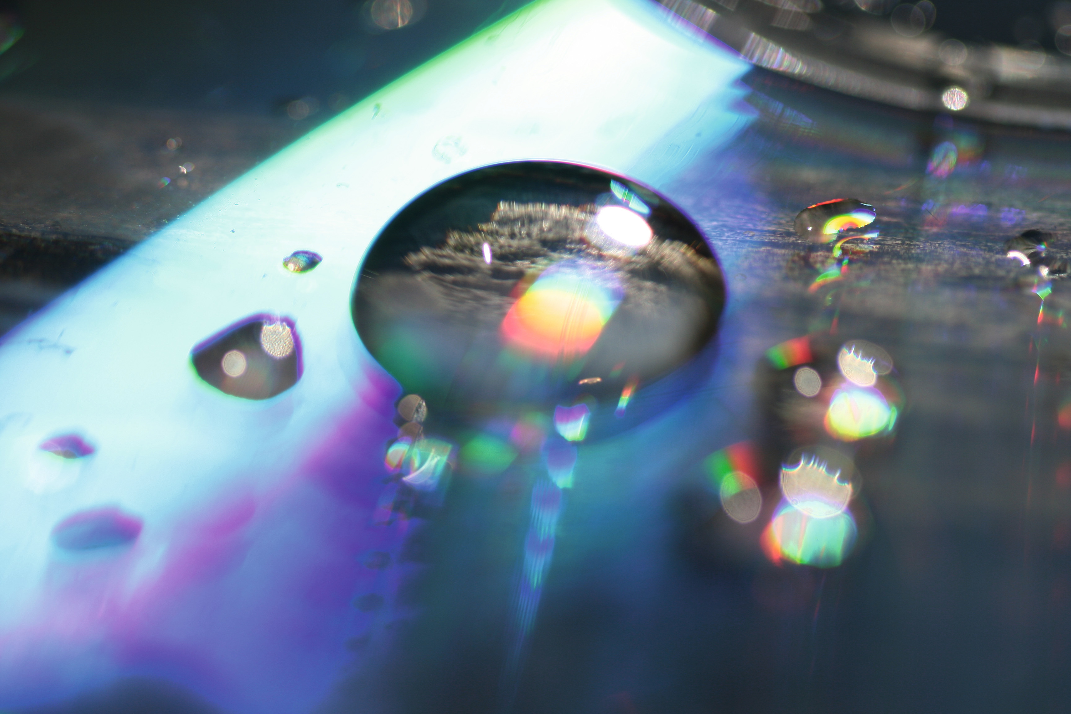
The lotus effect
In 1982 Willhelm Barthlott, botanist of Bonn University, through the electron microscope use, discovered why the lotus plant leaves seem to be self-cleaning. The reason depends on the leave surface, which is not smooth but, as it was called, Nano-rough, i.e. provided with invisible and tiny reliefs preventing liquids and filth from adhering to the surface of the leave itself. Today we speak of lotus effect. Over the years, botanists have studied the interesting properties of the lotus flower: the capability of not retaining water, due to the particular topology of the leave surface that lets water “slide away “, under the form of drops that, in their motion, leaves traces of mud, insects and so on, keeping the surface clean. The design and manufacture of new forefront materials and technological solutions draws inspiration from lotus leaves that, thanks to their nanostructure, are super-hydrophobic and self-cleaning.


